Square to Sine Wave Converter
Introduction
The purpose of this project is to design, build, fabricate, and test an op-amp based circuit that converts a 2Vpp at 350Hz square wave to a 4Vpp at 350Hz sine wave. The design leverages an active narrowband bandpass filter and the fundamental frequency component of the Fourier series of the input signal to filter out and amplify the sine wave. Because an inverting op-amp circuit is used, the filtered signal is cascaded into a second inverting op-amp to keep the output signal in phase with the input.
Design Details
To convert the input signal to a sine wave, a Fourier series expansion of the input square signal was used as shown below.
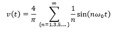
The fundamental frequency, or first harmonic, gives a sine wave of the original frequency in phase with the square wave.
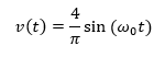
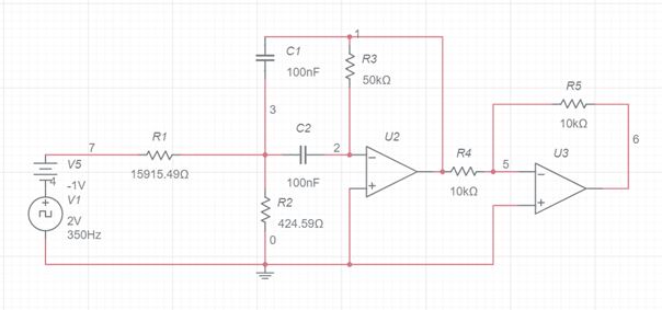
Thus, isolating the fundamental frequency results in a sine wave. To do this, an active narrowband bandpass filter was used with a center frequency of 350 Hz. A Multisim schematic of the filter is shown below as everything up to the resistor R4.
After deriving the transfer function, the gain K_0, bandwidth β, and center frequency ω_0 can be determined as follows. Note that the total gain of the input will include the 4/π from the Fourier expansion.
Therefore, the resistor and capacitor values shown in in the schematic create a bandpass filter centered at 350 Hz, the fundamental frequency of the input square wave, with a gain of 2, and a narrow passband of 400 rad/s. After R4, the schematic shows a second op amp used as an inverting amplifier with a gain of 1. Cascading the bandpass filter into the inverting amplifier results in a noninverted output.
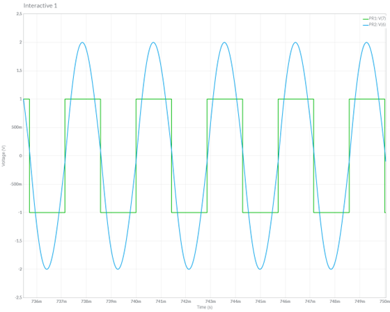
With the design complete and the component values chosen, the circuit was simulated in Multisim. The output shown below depicts a 2 Vpp 350 Hz square wave input converted to a 4 Vpp 350 Hz sine wave output in phase with the input square wave.
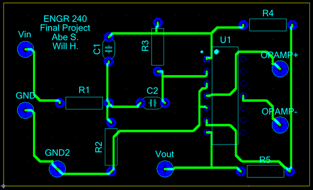
After simulating, the circuit was transferred to a PCB layout in Ultiboard, shown below, and sent to be fabricated. For the op amps, the LM348 from Texas Instruments was chosen for the convenience of multiple op amps on one IC. The LM348 can be seen as U1 in the PCB layout. Once the PCB was fabricated all there was left to do was assemble and test.

Results and Discussion
Upon receiving and populating the PCB, the circuit was tested with the input 2 Vpp 350 Hz square wave at Vin, expecting a 4 Vpp 350 Hz sine wave in phase with the square wave at Vout. Using an oscilloscope, the output was confirmed to be as expected, shown below. Vin is in yellow and Vout is in blue.

Due to limited instrument precision, the input Vin signal is not exactly as described. However, 2.04 Vpp at 349.6 Hz showing a square wave is within the appropriate error margin for this project. The output errors are caused again by limited instrument precision, as well as imperfections within the resistor and capacitor values, the op amps, and PCB used in the circuit. For this reason, the output comes out as a 4.16 Vpp at 349.6 Hz sine wave with a 3.776° phase shift from the input square wave.
Conclusion
The circuit fulfilled the purpose of this project. Improvements to the circuit itself could be made using higher quality components with less error. The PCB in this project was designed to resemble the circuit layout but could be made much smaller by removing empty space and orienting all components for space rather than readability. Additionally, the LM348 chip used for the op amps in this design houses four op amps, though the circuit only needs two. Using a chip with only two op amps may provide cost and space savings.